Are you ready to stand out in your next interview? Understanding and preparing for Component Placement and Inspection interview questions is a game-changer. In this blog, we’ve compiled key questions and expert advice to help you showcase your skills with confidence and precision. Let’s get started on your journey to acing the interview.
Questions Asked in Component Placement and Inspection Interview
Q 1. Explain the process of component placement in PCB assembly.
Component placement in PCB (Printed Circuit Board) assembly is the crucial process of precisely positioning and attaching electronic components onto the PCB. Think of it like arranging intricate puzzle pieces on a board, each needing to be in the exact right spot to ensure the circuit functions correctly. This process involves several steps, starting with the preparation of the PCB and components. Then, a placement machine picks up each component, guided by the PCB’s design data, and places it on the designated pad with high accuracy. Finally, the components are secured through reflow soldering, where the PCB is heated to melt the solder paste, bonding the components firmly. The whole process is automated for efficiency and precision, minimizing human error.
For instance, imagine assembling a smartphone’s motherboard. Thousands of tiny components, like resistors, capacitors, and integrated circuits, need precise placement; even a slight misalignment can render the entire device dysfunctional. Therefore, the accuracy and speed of this process are paramount in the manufacturing of electronic devices.
Q 2. Describe different types of component placement machines.
Component placement machines vary significantly in their capabilities and technology. The most common types include:
- Pick-and-place machines: These are the workhorses of the industry, utilizing robotic arms to pick components from feeders and place them on the PCB. They range from simple, low-speed machines for small-batch production to high-speed, multi-headed machines for mass production. These machines offer flexibility, accommodating a wide range of component types and sizes.
- Chip shooters: These machines are specialized for placing surface-mount components (SMD) very efficiently. They use compressed air to ‘shoot’ small components onto the PCB at high speed. They are ideal for high-volume production of boards with many small components.
- Hybrid machines: These machines combine the features of pick-and-place and chip shooter technology, providing maximum flexibility and speed. They can handle a wide range of components, from small chips to large connectors.
The choice of machine depends heavily on production volume, component types, and budget. For example, a small electronics prototyping shop might use a simple pick-and-place machine, while a large-scale manufacturer of smartphones would invest in high-speed, hybrid machines for optimal efficiency.
Q 3. What are the common challenges in component placement?
Component placement is a challenging process fraught with potential issues. Some of the common challenges include:
- Component damage: Sensitive components can be easily damaged during the handling and placement process. This can lead to malfunctions or complete failure of the PCB.
- Misplacement: Incorrect placement, even by a fraction of a millimeter, can result in shorts, opens, or other circuit errors.
- Component orientation errors: Many components need to be oriented correctly for proper function. Incorrect orientation can cause malfunctions.
- Feed issues: Problems with component feeders can cause delays and lead to placement errors. Empty feeders, jammed feeders, or incorrect feeder settings can disrupt the process.
- Machine calibration and maintenance: Poorly calibrated or poorly maintained machines can lead to significant inaccuracies in placement.
Addressing these challenges requires meticulous planning, process control, and rigorous quality checks throughout the assembly process.
Q 4. How do you ensure accurate component placement?
Ensuring accurate component placement relies on a multi-faceted approach:
- Precise machine calibration: Regularly calibrating placement machines is crucial to maintain accuracy. This involves checking the machine’s alignment, speed, and pressure settings.
- Accurate component feeding: Using appropriate feeders and ensuring they are properly filled and maintained is vital. Incorrect component orientation in the feeder can lead to placement errors.
- High-quality PCB design: A well-designed PCB with clearly defined component footprints and adequate spacing minimizes placement challenges.
- Use of vision systems: Many modern machines incorporate vision systems that verify component placement in real-time. These systems can detect and correct errors before they lead to further problems.
- Process monitoring and control: Close monitoring of the placement process using Statistical Process Control (SPC) techniques can help to identify and address potential issues before they escalate.
Think of it like a skilled surgeon performing a delicate operation – every step must be precise and controlled to ensure a successful outcome. Regular maintenance and calibration are essential to prevent errors and ensure high-quality results.
Q 5. What are the different types of inspection methods used in PCB assembly?
Several inspection methods are employed to verify the quality of PCB assembly. These include:
- Automated Optical Inspection (AOI): This is the most common method, using cameras and sophisticated image processing software to inspect for placement errors, component orientation errors, and solder defects.
- Manual visual inspection: While less efficient for high-volume production, visual inspection by trained technicians remains valuable, especially for detecting complex defects that are challenging for AOI to identify.
- X-ray inspection: This technique uses X-rays to inspect components and solder joints underneath other components, identifying hidden defects.
- Electrical testing: This method tests the functionality of the assembled PCB using various testing equipment. It verifies that the circuit operates as designed.
Each method has its strengths and limitations, and often a combination of techniques is used to provide comprehensive quality control.
Q 6. Explain the role of Automated Optical Inspection (AOI) in PCB assembly.
Automated Optical Inspection (AOI) plays a critical role in ensuring the quality and reliability of PCB assemblies. It’s an automated, non-destructive inspection method that uses cameras and sophisticated software to identify defects such as:
- Component placement errors: Incorrect X, Y, and θ (rotation) coordinates of components.
- Missing components: Identifying empty pads or missing components altogether.
- Component orientation errors: Incorrectly oriented components.
- Solder defects: Excessive solder, insufficient solder, bridging, or tombstoning.
AOI significantly increases efficiency and reduces the likelihood of defective products reaching the end-user. Imagine a factory producing thousands of PCBs daily; manual inspection would be incredibly time-consuming and prone to human error. AOI provides a fast, objective, and consistent inspection process, leading to improved quality control and reduced costs.
Q 7. How do you interpret AOI reports?
Interpreting AOI reports requires understanding the software and its output. Typically, an AOI report will include:
- Images of defects: High-resolution images highlighting the location and type of defects.
- Defect classification: Categorization of defects (e.g., missing component, incorrect orientation, solder bridging).
- Defect severity: Indication of the severity of the defect (e.g., critical, major, minor).
- Statistical summary: Overall defect rates and trends.
A skilled technician can use this information to pinpoint areas of concern in the production process. For example, a high rate of missing components might indicate a problem with the component feeder. Similarly, a high rate of solder bridging might suggest issues with the reflow soldering process. The report guides corrective actions to improve the assembly process and reduce defect rates.
Q 8. What are the common defects found during PCB inspection?
Common defects during PCB inspection span several categories. Think of it like a detective examining a crime scene; you’re looking for inconsistencies that could lead to malfunctions.
- Soldering Defects: These are very common and include bridges (excess solder connecting adjacent pads), cold solder joints (poor connection due to insufficient heat), tombstoning (one end of a component lifting off the board during reflow), and insufficient solder (resulting in a weak connection). Imagine a wobbly chair – a cold solder joint is like a leg not properly attached.
- Component Placement Errors: Incorrect placement can range from slight misalignment to completely wrong locations. This can lead to short circuits or components not functioning as intended. Picture assembling a puzzle where a piece is in the wrong spot—the whole picture is disrupted.
- Mechanical Damage: This includes bent leads, cracked components, or physical damage to the board itself. Imagine a dropped phone with a cracked screen; similarly, physical stress can ruin a PCB.
- Missing Components: Simply put, a component that should be there, isn’t. This is a critical error that can completely halt functionality.
- Polarity Errors: Certain components (like electrolytic capacitors or diodes) have a defined polarity. Reversing them leads to immediate failure. It’s like installing a battery backward in a device.
Identifying these defects requires a keen eye and often involves using magnification tools and automated optical inspection (AOI) systems.
Q 9. Describe your experience with soldering techniques.
My experience with soldering encompasses both through-hole and surface mount technologies. I’m proficient in various soldering techniques, including manual soldering with irons (using different tip sizes and fluxes depending on the component), wave soldering (for through-hole components), and reflow soldering (for surface mount components). I understand the importance of proper temperature control, flux application, and post-soldering inspection. I’ve also worked extensively with specialized soldering equipment, such as hot air rework stations and precision soldering robots, to ensure optimal solder joints.
For instance, while working on a high-frequency circuit board, I successfully utilized a specialized low-temperature solder paste and a controlled reflow profile to avoid damaging sensitive components. Careful temperature profiling is like baking a cake – too much heat, and you’ll burn it; too little, and it won’t cook properly.
Q 10. How do you troubleshoot component placement errors?
Troubleshooting component placement errors starts with a systematic approach. First, I compare the actual placement against the design using the Gerber files or CAD data. This is my blueprint. Next, I use AOI (Automated Optical Inspection) results to pinpoint the exact location and type of error. If these tools identify potential issues, I conduct manual verification under magnification. Common root causes include misaligned pick-and-place machine nozzles, incorrect component feeder settings, or errors in the PCB design itself.
Let’s say AOI flags several components as misaligned. I’d check the nozzle alignment on the pick-and-place machine, verify the component footprints in the design software, and potentially re-run the assembly process with corrected settings. It’s like fixing a typo; you need to locate the error, understand why it happened, and then correct it.
Q 11. What are the quality standards you follow in component placement and inspection?
I strictly adhere to IPC-A-610 for acceptability of electronic assemblies and IPC-7711/7721 for soldering. These standards provide a detailed classification of acceptable and unacceptable defects. Beyond these, I incorporate statistical process control (SPC) methodologies to track and analyze process capabilities. We employ statistical tools like control charts to monitor key process parameters, ensuring that our component placement and soldering processes remain within predefined limits. This ensures consistent, high-quality results. Think of it as a quality control system that helps us prevent defects rather than just find them.
Further, our company’s internal quality management system complements these standards, emphasizing continuous improvement through regular audits and operator training.
Q 12. Explain the importance of IPC standards in PCB assembly.
IPC standards, such as IPC-A-610 and IPC-J-STD-001, are crucial for consistent quality in PCB assembly. They provide a common language and criteria for evaluating the quality of electronic assemblies across the industry. They establish clear acceptance criteria for various aspects of PCB assembly, including component placement, soldering, and cleanliness. This facilitates communication and collaboration between manufacturers, designers, and customers. It’s like a universal measuring system; everyone knows what constitutes a ‘good’ product.
These standards promote consistency, reduce failures, and ensure the reliability and longevity of electronic products, significantly impacting manufacturing processes and reducing waste.
Q 13. How do you handle discrepancies between design specifications and actual placement?
Discrepancies between design specifications and actual placement require immediate attention. First, I identify the source of the discrepancy: Was it a design error, a manufacturing error, or a mismatch in the assembly process? Then, I gather evidence—comparing the Gerber files, the BOM (Bill of Materials), and the actual PCB layout. I meticulously document the findings and communicate them to the relevant stakeholders (design engineers, production managers). A collaborative approach is essential to find a solution, whether it’s correcting the design, adjusting the manufacturing process, or implementing rework procedures.
For example, if a component’s placement is slightly off, we’d assess whether it impacts functionality. If it does, we might need rework; if not, we might document it as a minor deviation with justification for acceptance.
Q 14. What is your experience with different types of components (e.g., through-hole, surface mount)?
I have extensive experience handling both through-hole and surface mount components. My experience includes working with a broad range of components including passive components (resistors, capacitors, inductors), integrated circuits (ICs), connectors, and active components (transistors, diodes). I’m familiar with various component sizes and packages (e.g., SOIC, QFN, BGA) and the unique handling requirements each entails.
For example, handling BGAs (Ball Grid Arrays) requires specialized equipment and techniques due to their small pitch and delicate solder balls. Through-hole components demand a different approach, emphasizing correct lead forming and ensuring proper solder joint creation.
Q 15. Describe your experience with different PCB assembly processes.
My experience encompasses a wide range of PCB assembly processes, from manual to automated techniques. I’ve worked extensively with through-hole technology (THT), where components are inserted into holes drilled in the PCB and soldered, and surface mount technology (SMT), where components are placed directly onto the surface of the board. In SMT, I’m proficient in various placement methods including pick-and-place machines, both high-speed and selective, and manual placement for smaller, specialized runs or repairs. I’m also familiar with reflow soldering techniques, including convection, infrared, and vapor phase reflow. I’ve managed projects using wave soldering for THT components. Understanding the nuances of each process is critical to ensuring optimal quality and efficiency.
For example, I once managed a project involving both THT and SMT components, requiring careful coordination of different assembly lines and quality control checkpoints. We used a combination of automated and manual processes to optimize the workflow and meet tight deadlines.
Career Expert Tips:
- Ace those interviews! Prepare effectively by reviewing the Top 50 Most Common Interview Questions on ResumeGemini.
- Navigate your job search with confidence! Explore a wide range of Career Tips on ResumeGemini. Learn about common challenges and recommendations to overcome them.
- Craft the perfect resume! Master the Art of Resume Writing with ResumeGemini’s guide. Showcase your unique qualifications and achievements effectively.
- Don’t miss out on holiday savings! Build your dream resume with ResumeGemini’s ATS optimized templates.
Q 16. How do you maintain cleanliness and organization in your workspace?
Maintaining a clean and organized workspace is paramount for efficiency and preventing defects. I follow a 5S methodology (Sort, Set in Order, Shine, Standardize, Sustain) rigorously. This involves regularly sorting components and tools, arranging them in a logical order for easy access, thoroughly cleaning the workspace, standardizing our procedures, and maintaining these standards consistently. We also utilize designated areas for different tasks, such as component preparation, placement, inspection, and rework, and regularly use ESD mats and equipment to prevent static damage.
Think of it like a well-stocked kitchen – you can’t cook efficiently if everything is scattered. A clean and organized workspace streamlines the process, leading to fewer errors and faster turnaround times. This approach significantly reduces the risk of component misplacement or damage and makes it easier to identify and rectify any issues promptly.
Q 17. Explain your experience with statistical process control (SPC).
Statistical Process Control (SPC) is integral to maintaining consistent quality in PCB assembly. I’m experienced in using control charts, such as X-bar and R charts, to monitor key process variables, including component placement accuracy, solder joint quality, and defect rates. These charts help identify trends and potential problems before they escalate into major issues. I’ve used SPC data to make informed decisions about process adjustments, such as fine-tuning the placement machine parameters or adjusting the reflow profile, resulting in significant improvements in yield and quality.
For instance, we used SPC to track the placement accuracy of a specific component. When we noticed an upward trend in deviations outside the control limits, we investigated and discovered a slight misalignment in the placement head. By correcting the alignment, we brought the process back into control and reduced the defect rate significantly.
Q 18. How do you manage your time effectively to meet production deadlines?
Effective time management is crucial in meeting production deadlines. I employ several strategies, including meticulous planning, prioritizing tasks based on urgency and importance, and using project management tools to track progress. I regularly communicate with the team, keeping everyone informed of potential delays and coordinating efforts to address challenges proactively. I utilize time-tracking software to identify bottlenecks and optimize workflow efficiency. Breaking down large tasks into smaller, manageable sub-tasks also helps in staying on schedule and maintaining focus.
In one high-pressure project, we utilized a Kanban system to visually track the flow of work and identify any delays. This allowed us to redistribute workload effectively, ensuring we met the tight deadline.
Q 19. What is your experience with different types of inspection tools and equipment?
My experience with inspection tools and equipment includes a wide range of instruments. I’m proficient in using optical microscopes for detailed solder joint inspection, automated optical inspection (AOI) systems for rapid detection of defects in high-volume production, X-ray inspection systems for identifying hidden defects beneath components, and various manual gauging tools for measuring component placement accuracy. I’m also trained in using specialized equipment such as a solder paste inspection (SPI) machine to ensure proper paste deposition.
The choice of inspection tools depends heavily on the complexity of the PCB and the required level of detail. For example, AOI is ideal for high-throughput screening, but microscopy is necessary for thorough examination of intricate solder joints.
Q 20. How do you handle high-volume production requirements?
Handling high-volume production requires a structured approach, focusing on efficiency, automation, and robust quality control systems. I have experience optimizing automated placement machines for maximum throughput, implementing efficient material handling systems, and utilizing statistical process control to maintain consistent quality. Lean manufacturing principles, such as minimizing waste and maximizing value, are critical in this context. Training personnel effectively is also essential to ensure consistent performance and minimize errors. Regular maintenance of equipment is also crucial to prevent unexpected downtime and delays.
In one project involving millions of units, we implemented a just-in-time inventory system to minimize storage space and optimize material flow, coupled with rigorous quality checks at each stage of the production line. This significantly improved efficiency and allowed us to meet the high-volume requirements without compromising quality.
Q 21. Describe your experience working with different types of solder pastes.
My experience with solder pastes includes various types, each with unique properties suited for specific applications. I’m familiar with lead-free and leaded solder pastes, different alloy compositions (e.g., SAC305, Sn63Pb37), and varying viscosities (tackiness) which influence printing and placement accuracy. I understand the importance of selecting the appropriate paste type based on component size, board design, and the reflow process used. Proper handling and storage of solder paste is vital, to prevent degradation and ensure consistent performance. Improper storage can lead to changes in viscosity, adversely affecting printing and solder joint quality.
For instance, I’ve used a low-viscosity paste for fine-pitch components to ensure proper dispensing, and a higher viscosity paste for larger components to prevent slumping or sagging before reflow. This selection was critical in achieving optimal solder joints and avoiding defects.
Q 22. Explain your understanding of reflow soldering profiles.
A reflow soldering profile is a precisely controlled temperature curve that dictates how a printed circuit board (PCB) is heated during the soldering process. It’s crucial for achieving reliable solder joints. Think of it as a recipe for perfectly melting solder – if you don’t follow it correctly, your solder joints might be weak or even fail completely.
A typical profile includes several key stages:
- Preheating: The PCB is gradually heated to a specific temperature, typically around 100-150°C. This helps to equalize the temperature across the board and prevent thermal shock to sensitive components.
- Soak Zone: The board is held at a constant temperature for a defined period. This allows the solder paste to properly flow and evenly wet the component leads and PCB pads.
- Reflow Zone: The temperature is rapidly increased to the peak reflow temperature (typically around 217-230°C for lead-free solder), melting the solder paste and forming solder joints. This is the most critical stage.
- Cooling Zone: The PCB is slowly cooled down to allow the solder joints to solidify and prevent cracking. Too rapid cooling can lead to poor solder joint formation.
Different components have different thermal profiles; therefore, optimizing the reflow profile is critical to avoid component damage. For instance, sensitive components like high-precision quartz crystals might require gentler heating and cooling ramps than more robust components. Incorrect reflow profiles can lead to various defects, including cold solder joints, tombstoning, head-in-pillow, and solder bridging.
Q 23. How do you address component misalignment or placement errors?
Component misalignment or placement errors are addressed through a combination of preventative measures and corrective actions. Prevention is always the best approach, but sometimes errors occur. When misalignments are detected, the first step is to assess the severity. Minor misalignments might be acceptable depending on the component and design tolerances. Significant errors, however, require corrective actions.
My strategies include:
- Visual Inspection: A thorough visual check using a microscope or magnification tools identifies misalignments immediately after placement.
- Automated Optical Inspection (AOI): AOI systems automatically detect misplacements and generate detailed reports. This is vital for high-volume production.
- Manual Correction (If Allowed): For minor misalignments and with certain components, manual adjustment might be possible. This must be done cautiously to avoid damaging components or the PCB. It’s often better to replace the component.
- Component Replacement: If manual correction is impossible or risky, the misaligned component is replaced with a new one, ensuring proper placement with the help of stencils, pick-and-place machines, or by hand if necessary.
Documentation is key. Every correction or replacement is meticulously recorded, including the nature of the error, the corrective action taken, and the component’s location. This data informs continuous improvement efforts.
Q 24. What are your strategies for preventing defects during component placement?
Preventing defects during component placement is paramount for ensuring high-quality PCBs. My strategies focus on meticulous planning and execution throughout the assembly process.
- Proper Stencil Design and Maintenance: Ensuring the stencil is correctly designed and free from damage prevents solder paste issues that can lead to misplacements.
- Optimized Solder Paste: Using the right type of solder paste with the appropriate viscosity is crucial for effective component wetting and placement.
- Accurate Pick-and-Place Machine Calibration and Maintenance: Regular calibration and maintenance of pick-and-place machines are necessary for accuracy and consistency.
- Cleanliness of the Work Environment: A clean workspace prevents contamination and improves placement accuracy. Any dust or debris can easily disrupt the placement process.
- Proper Handling of Components: Carefully handling sensitive components prevents damage and ensures accurate placement.
- Regular Process Audits: Frequent audits ensure adherence to standardized procedures, leading to fewer errors.
- Operator Training: Well-trained operators are more likely to identify and prevent errors before they happen. Regular training and cross-training enhance the skill set of the whole team.
By meticulously following these strategies, the chance of defects dramatically decreases. Remember, prevention is far more efficient and cost-effective than correction.
Q 25. How do you document and report inspection findings?
Inspection findings are documented and reported using a combination of methods tailored to the specific needs of the project. The goal is to provide clear, concise, and actionable information.
- Inspection Reports: Detailed reports include the date, time, inspector’s name, PCB identification, list of defects, location of defects, severity level (minor, major, critical), and images or videos documenting the defects. These reports often use standardized forms for consistency.
- Defect Tracking Systems: Sophisticated software systems track defects and provide statistical data on common issues, allowing for efficient root-cause analysis and process improvements. This enables better decision-making on potential process modifications.
- Visual Aids: Images and videos are invaluable in providing visual context for defects, especially for complex assemblies. Clear, well-lit pictures can save a lot of time and misunderstandings.
- Statistical Process Control (SPC) Charts: SPC charts track key metrics like defect rates over time. These charts assist in identifying trends and help implement corrective actions proactively.
The reporting method must be chosen based on company protocols and the complexity of the project. The key is clear communication—the reports need to be easily understood by all stakeholders, from production staff to quality control managers.
Q 26. What are the safety precautions you observe during PCB assembly?
Safety is of utmost importance during PCB assembly. My adherence to safety procedures always comes first. This includes:
- ESD Precautions: Electrostatic discharge (ESD) can damage sensitive components. I always use proper ESD equipment, including wrist straps and mats, and ensure the workspace is grounded.
- Eye Protection: Safety glasses or goggles are used to protect my eyes from potential hazards like solder splashes or flying debris.
- Proper Ventilation: Soldering fumes can be harmful. Adequate ventilation ensures a safe working environment. This includes the use of fume extractors if necessary.
- Personal Protective Equipment (PPE): Gloves are usually worn to protect skin from chemicals and soldering materials.
- Machine Safety: Adhering to all machine safety protocols, including emergency stops and proper machine guarding, is critical when working with automated equipment.
- Proper Disposal of Hazardous Materials: Solder and cleaning materials are disposed of following all applicable safety regulations and environmental guidelines.
Regular safety training and refresher courses reinforce safe practices and ensure awareness of potential hazards.
Q 27. Describe your experience working with a team in a manufacturing environment.
I thrive in team environments. In my previous role, I collaborated closely with a team of engineers, technicians, and quality control inspectors in a fast-paced manufacturing setting. Our shared goal was to achieve high-quality production while maintaining efficiency and adhering to strict deadlines.
My contributions included:
- Process Optimization: I actively participated in identifying bottlenecks and streamlining processes. This involved close collaboration with the engineering team, leading to reduced lead times and improved efficiency.
- Troubleshooting: I worked collaboratively to troubleshoot production issues, sharing my expertise to identify root causes and implement effective solutions.
- Knowledge Sharing: I regularly shared my knowledge with team members, providing training and guidance to enhance their skills and improve the overall team performance. This includes mentoring junior technicians in best practices.
- Effective Communication: I prioritized clear and concise communication with all team members, ensuring that information was effectively shared and potential problems were addressed promptly.
My team experience has taught me the importance of collaboration, communication, and mutual respect in achieving shared goals.
Q 28. How do you stay updated on the latest advancements in component placement technology?
Staying updated on the latest advancements in component placement technology is crucial for maintaining my expertise and ensuring efficient processes. I utilize several methods:
- Industry Publications and Journals: I regularly read trade publications and journals focused on electronics manufacturing to stay informed about the latest trends and technologies.
- Conferences and Trade Shows: Attending conferences and trade shows offers firsthand experience with new equipment and allows networking with industry leaders.
- Online Resources and Webinars: I actively participate in online forums and utilize webinars and online courses offered by equipment manufacturers and industry experts.
- Manufacturer’s Websites and Documentation: Keeping up-to-date with manufacturers’ websites and documentation helps to understand the capabilities of new and existing equipment.
- Professional Organizations: Participating in professional organizations provides access to specialized knowledge, networking opportunities, and continuing education.
Continuous learning is integral to my professional development. By actively seeking new information, I ensure that my skills and knowledge remain relevant and competitive in this ever-evolving field.
Key Topics to Learn for Component Placement and Inspection Interview
- Understanding Component Specifications: Thoroughly review tolerance levels, material properties, and any relevant industry standards for components. Practice interpreting technical drawings and specifications.
- Placement Techniques and Methodologies: Familiarize yourself with various component placement methods (e.g., manual, automated, robotic) and their applications. Understand the importance of precision and accuracy in placement.
- Inspection Methods and Tools: Master different inspection techniques, including visual inspection, dimensional measurement (calipers, micrometers), and automated optical inspection (AOI). Know the strengths and limitations of each method.
- Quality Control and Statistical Process Control (SPC): Understand the principles of quality control and how SPC charts are used to monitor and improve the placement and inspection process. Be prepared to discuss process capability and control limits.
- Troubleshooting and Problem-Solving: Practice identifying and resolving common issues encountered during component placement and inspection. Develop your ability to analyze data, identify root causes, and propose effective solutions.
- Safety Procedures and Regulations: Demonstrate a strong understanding of relevant safety protocols and regulations related to handling components and operating inspection equipment.
- Documentation and Reporting: Understand the importance of accurate record-keeping, including documenting inspection results and reporting any defects or non-conformances.
Next Steps
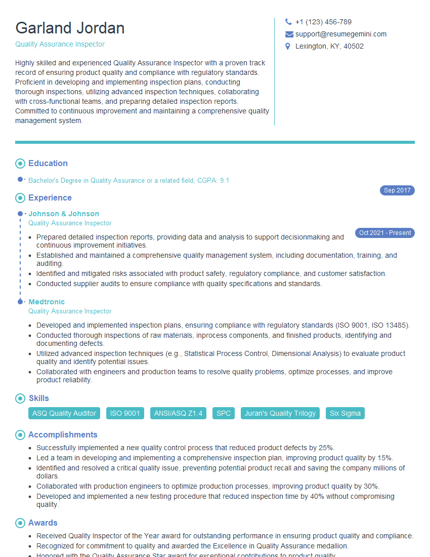
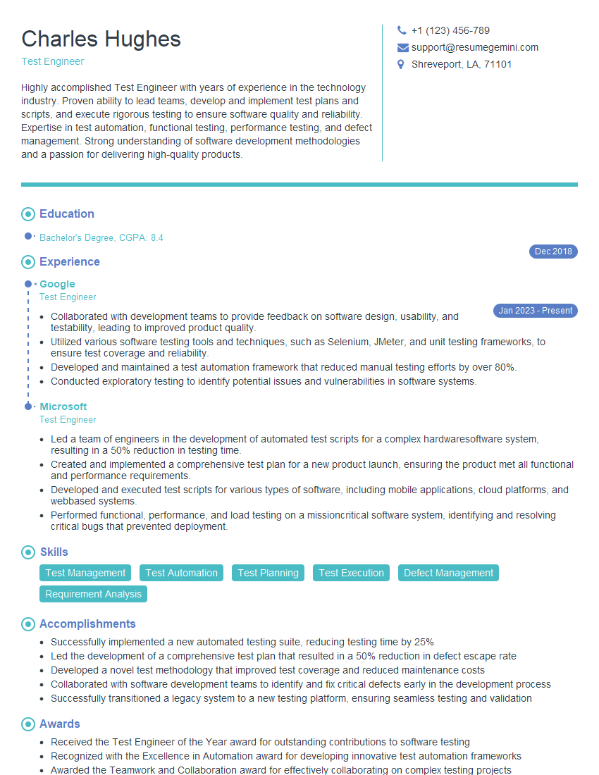
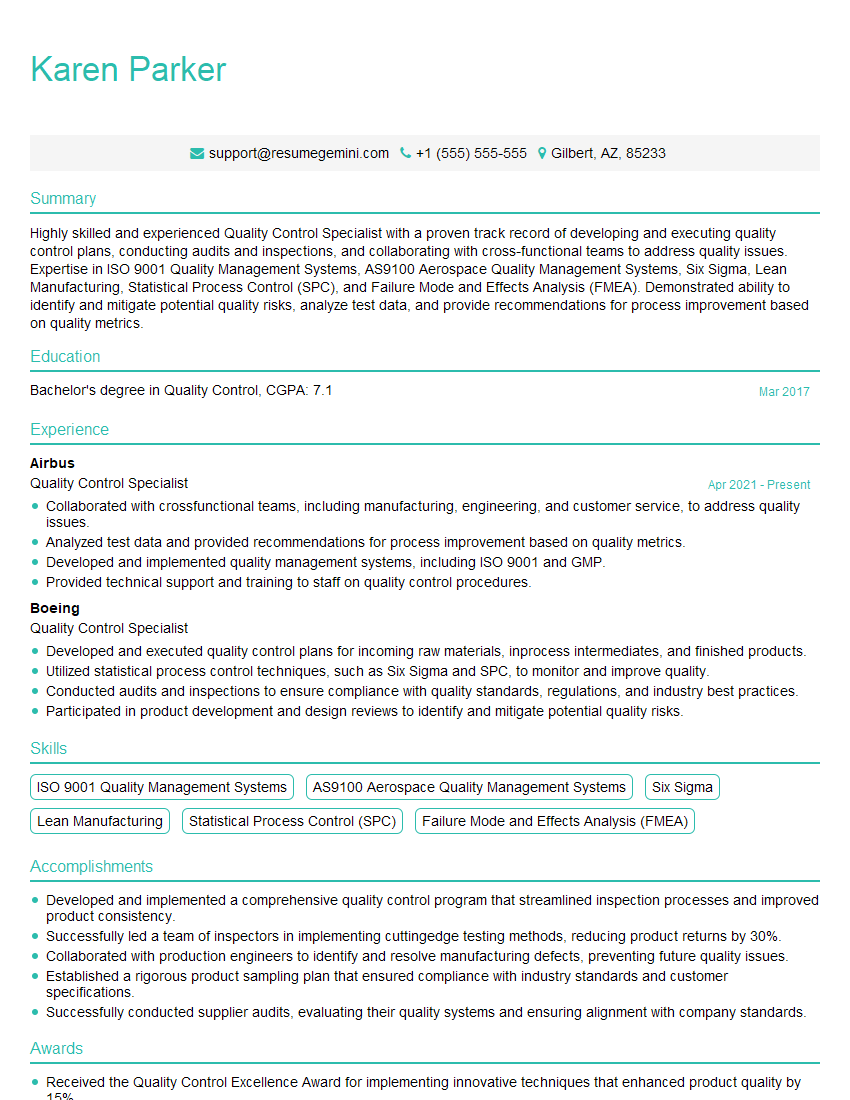
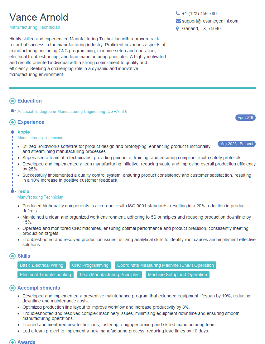
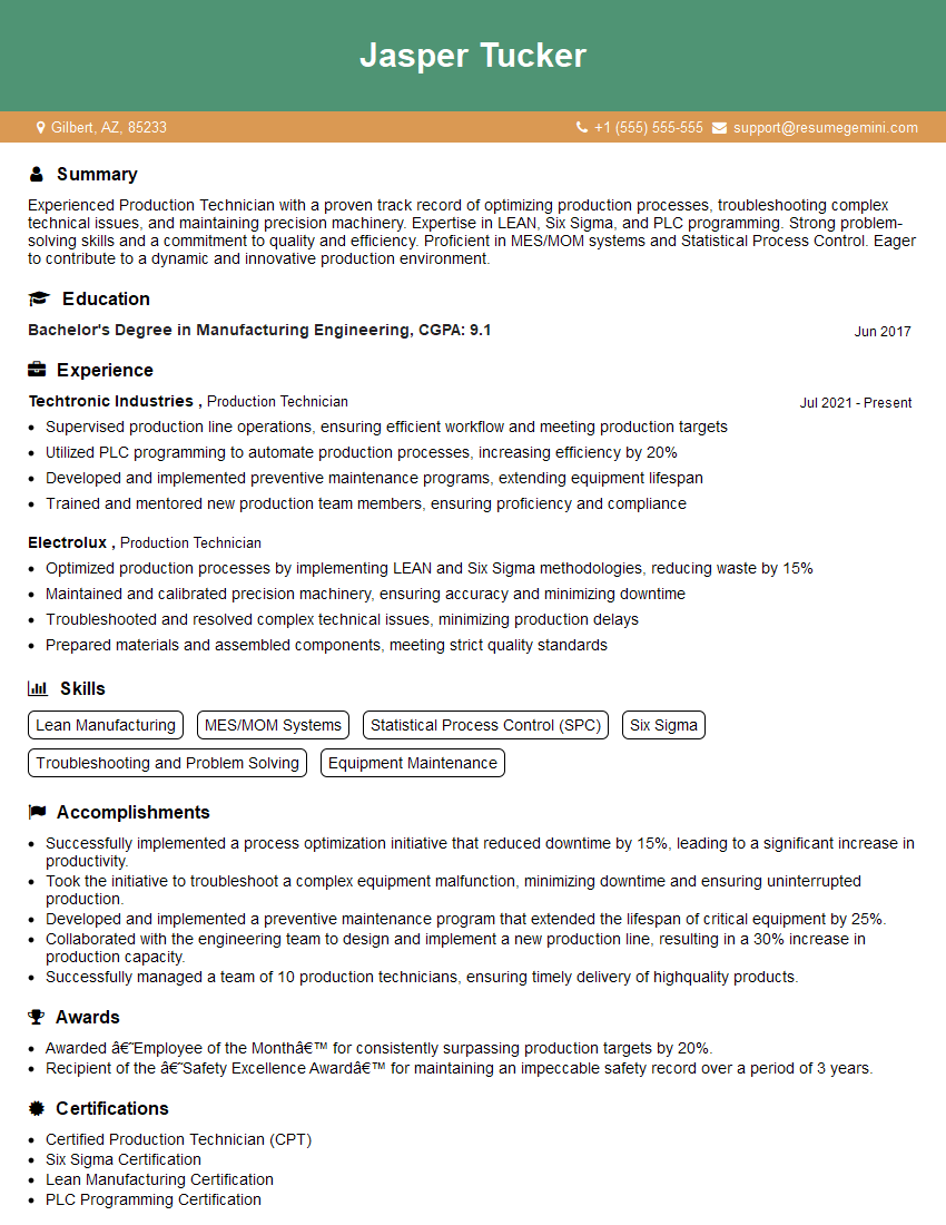
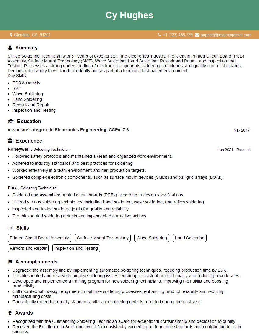
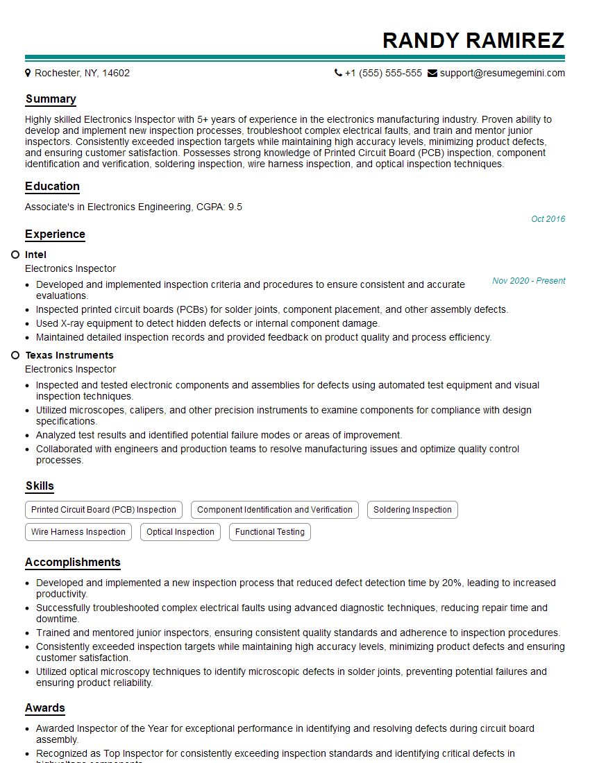
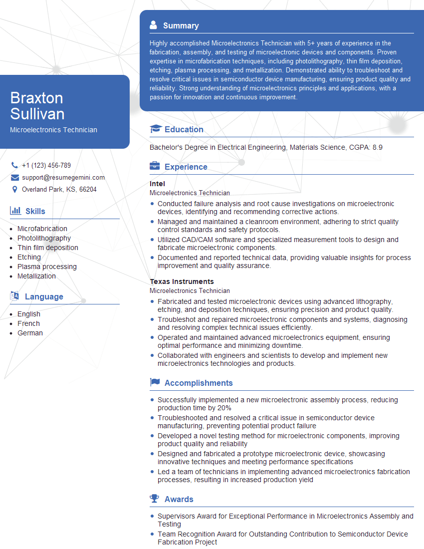
Mastering Component Placement and Inspection opens doors to rewarding careers in manufacturing, electronics, and various other high-tech industries. These skills are highly sought after, and demonstrating proficiency can significantly advance your career prospects. To make the most of your job search, creating an ATS-friendly resume is crucial. A well-crafted resume ensures your qualifications are highlighted effectively to hiring managers and Applicant Tracking Systems. We strongly recommend leveraging ResumeGemini to build a professional and impactful resume that showcases your expertise in Component Placement and Inspection. ResumeGemini provides examples of resumes tailored to this specific field, guiding you toward creating a document that gets noticed.
Explore more articles
Users Rating of Our Blogs
Share Your Experience
We value your feedback! Please rate our content and share your thoughts (optional).
What Readers Say About Our Blog
Hi, I have something for you and recorded a quick Loom video to show the kind of value I can bring to you.
Even if we don’t work together, I’m confident you’ll take away something valuable and learn a few new ideas.
Here’s the link: https://bit.ly/loom-video-daniel
Would love your thoughts after watching!
– Daniel
This was kind of a unique content I found around the specialized skills. Very helpful questions and good detailed answers.
Very Helpful blog, thank you Interviewgemini team.
